Semiconductor Devices • Process Development • RF/mmWave Engineering
Hands-on experience spanning ultrawide-bandgap semiconductor fabrication, radiation detectors, RF power-amplifier characterization, mmWave measurements, process optimization, and device development.
2021 2022 2024 - Present
●────────────────────────────●────────────────────────────●
TTU RFIC Lab Skyworks Solutions Center for Nanophotonics RF/mmWave Research RFIC Intern Graduate Research Assistant
GaN / 28 GHz RF PA Characterization h-BN / AlN:Zr
DPD / PA Testing GaN Doherty / pHEMT Semiconductor Fabrication Tape-out HFSS / Thermal Analysis Radiation Detection
Experience
✳︎
Experience ✳︎
Center for Nanophotonics Texas Tech University
Graduate Research Assistant
January 2024 – Present | Lubbock, TX
Skyworks Solutions
RFIC Intern June 2022 – December 2022 | Woburn, MA
Texas Tech RFIC Laboratory Texas Tech University
Graduate Research Assistant
June 2021 – August 2023 | Lubbock, TX
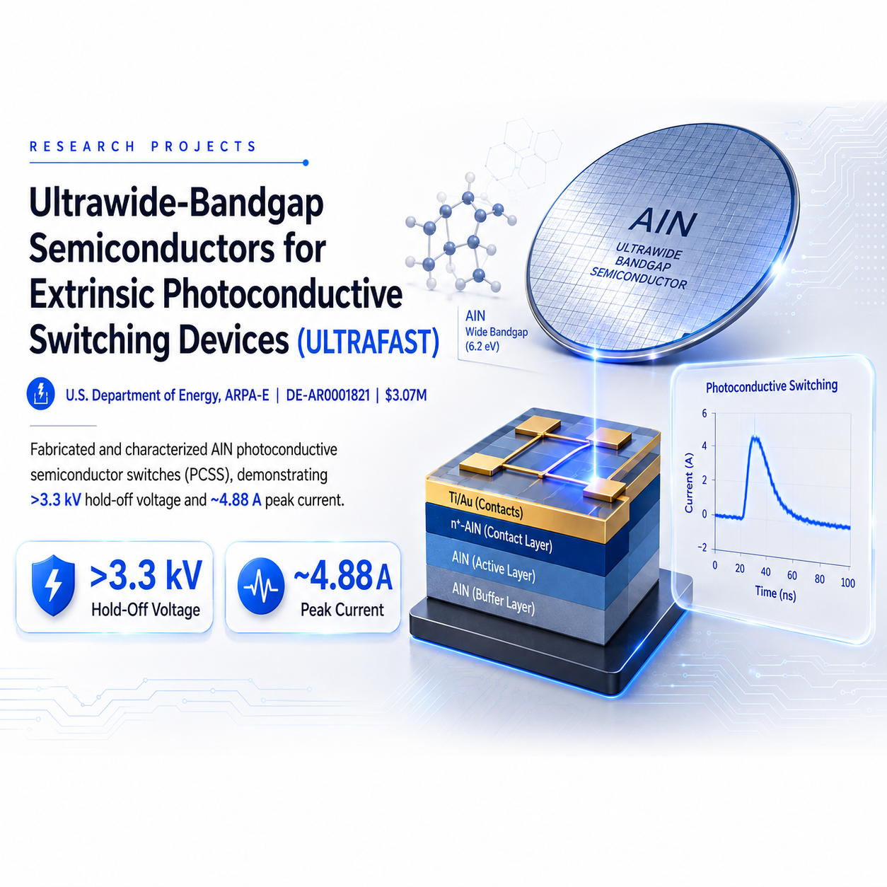
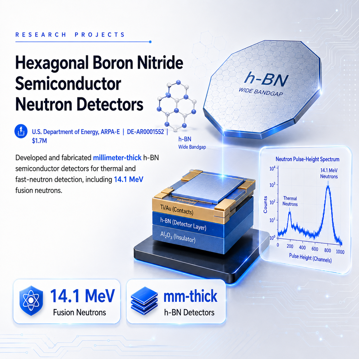
Developing ultrawide-bandgap semiconductor devices with emphasis on h-BN neutron detectors and AlN:Zr photoconductive semiconductor switches, covering device fabrication, process development, electrical/optical characterization, packaging, and performance optimization.
Developed millimeter-thick and multi-stacked h-BN semiconductor detectors for thermal and fast-neutron detection, including direct detection of 14.1 MeV D-T fusion neutrons.
Fabricated, packaged, and characterized h-BN radiation detectors using semiconductor processing, metal deposition, dry etching, wire bonding, and high-voltage electrical measurements.
Investigated charge-carrier transport and electrical/optical properties of thin and quasi-bulk h-BN and AlN:Zr ultrawide-bandgap semiconductor devices.
Designed and executed process-development experiments for h-BN by varying etch conditions, annealing temperature/time, metal/contact conditions, device geometry, photoresist/process conditions, laser power, and material thickness; correlated process parameters with electrical/optical device performance to identify optimized conditions and recommend process changes.
Troubleshot semiconductor fabrication processes and equipment, evaluated material/device performance across process splits, and documented experimental procedures, process conditions, results, and corrective actions for repeatable device fabrication.
Developed and tested AlN:Zr photoconductive semiconductor switch structures with >3.3 kV hold-off voltage and ~4.88 A peak current.
Installed, maintained, and troubleshot semiconductor fabrication and characterization equipment; translated completed research into peer-reviewed publications.
Semiconductor Fabrication
Mask aligner/ wafer processing
Photolithography
Dry etching
Metallization
Wire bonding
Device packaging
High-voltage device fabrication
Process Development
ICP etcher or process flow
Etch-condition optimization
Annealing temperature/time
Contact optimization
Photoresist/process conditions
Device geometry
Material thickness
Device Characterization
Keithley / optical setup
I–V characterization
Photocurrent
High-voltage measurements
Charge transport
Optical characterization
Performance comparison
Radiation Detection
h-BN detector or neutron setup
Thermal neutron detection
Fast neutron detection
14.1 MeV D-T neutrons
Pulse-height measurements
Charge collection
Detector-efficiency analysis
Performed characterization and analysis of wideband pHEMT and GaN Doherty RF power amplifiers, combining small- and large-signal measurements, linearity analysis, thermal characterization, and electromagnetic modeling
Performed Phase-II characterization of wideband pHEMT and GaN Doherty power amplifiers, including small-signal, large-signal, ACLR/DPD linearity, PAE, Psat, and IR thermal measurements
Performed HFSS electromagnetic analysis of cascaded EVB breakout/interconnect structures to evaluate transmission-line impedance.
Thermal Analysis and Temperature measurement on GaN Doherty & Wideband pHEMT Power Amplifier.
RF Power Amplifier Characterization
RF PA test setup
Small-signal characterization
Large-signal characterization
PAE
Psat
ACLR
DPD linearity
GaN & pHEMT Devices
RF module / GaN PA
Wideband pHEMT PA
GaN Doherty PA
Device-performance evaluation
Thermal Characterization
IR thermal camera
IR thermal measurements
Temperature characterization
GaN PA thermal analysis
Electromagnetic Modeling
HFSS field visualization
ANSYS HFSS
EVB interconnect analysis
Cascaded structures
Transmission-line impedance
Conducted RF and millimeter-wave power-amplifier characterization, device optimization, and IC-layout support while contributing to GaN-on-SiC and 28 GHz RFIC research
Assisted in tape outs by doing fill layout level.
Characterized 2-stack GaN-on-SiC power amplifiers and supported tape-outs through fill-layout work.
Tuned a 28 GHz GaAs stacked asymmetrical power combiner to >40% efficiency at P1dB; performed ACLR/DPD linearity, large-signal, and PAE measurements.
GaN-on-SiC Power Amplifiers
Characterized 2-stack GaN-on-SiC PAs
Large-signal measurements
PAE analysis
Linearity characterization
RF Linearity
ACLR
DPD
Large-signal testing
Efficiency analysis
IC Design Support
Fill-layout work
Tape-out support
Research Projects
✳︎
Research Projects ✳︎